
On April 23, 2025, the Ukrainian National Office for Intellectual Property and Innovations (UANIPIO) registered semiconductor product layouts for the first time in more than a decade. After a long pause in the receipt of applications for this intellectual property (until 2019 – topographies of integrated circuits), positive decisions were made on three applications filed by ND Production LLC.
These registrations mark the resumption of legal protection of semiconductor technologies in Ukraine. All three registered designs relate to controllers for electric charging stations (ECS), which are crucial elements of the electric transport infrastructure. This is not only a step towards strengthening the position of Ukrainian developers in the global market, but also a symbol of our country’s return to high standards of innovation in this area.
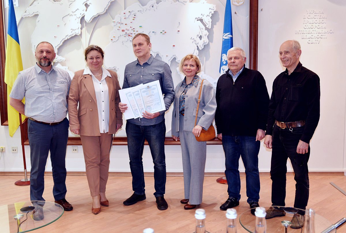
“This is a truly significant event for us. These are the first semi-conductor layout certificates issued in Ukraine after a long break”, – emphasized Olena Orliuk, Director of UANIPIO, during the presentation of the layout registration certificates to the applicant’s representatives and patent attorneys who supported the process: Leonid Cherepov and Tatiana Lisna.
“We are extremely pleased that Ukraine is returning to the topic of semiconductors, because we used to have a very powerful school and a high level of development in this area. This is not just a resumption of practice – it is the beginning of a new movement. I deeply appreciate the authors and inventors and sincerely thank the patent attorneys who supported this process. As part of our strategy to support innovation, we see the development of this IP right as one of our priorities”, – noted Olena Orliuk.
“Here, at UANIPIO we actively support the development of the semiconductor industry – not only at the stage of creation, but also at the stage of their commercialization. We expect new promising applications and believe that this case is of strategic importance for the victory and development of our country”, – said Ihor Parenchuk, Deputy Director of UANIPIO.
Yuriy Malyshev, a representative of the company that filled the layout design for registration and one of the authors of the device, noted that this event was significant for him as well:
“I have been keen on electronics since school days, designing and drawing circuit boards. In addition, today we have developments that are already superior in quality to Chinese and other analogues – we have orders from Europe, and we are proud of this. We want to preserve the Ukrainian name and work in Ukraine for Ukraine.”
“As a patent attorney, I have always wanted to ensure that the layouts in Ukraine are properly protected”, – emphasized Leonid Cherepov, “This case is an important signal to other developers: it is worth not only creating unique things but also protecting them. The revival of the registering practice of this intellectual property right is a powerful impetus for the entire industry.”
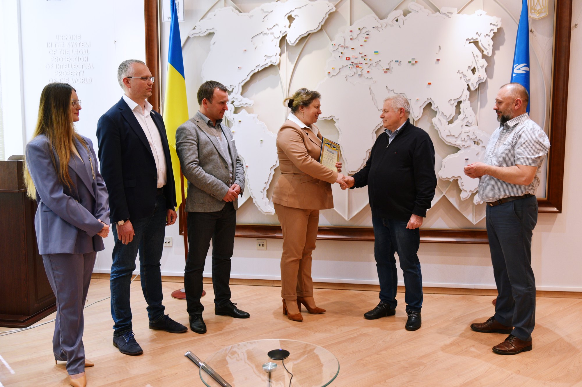
The IP Office management also presented Leonid Cherepov with a Certificate of Appreciation for his contribution to the development of intellectual property and innovation in Ukraine
For reference:
Layout of a semiconductor product (layout) is a set of related images, fixed or encoded in a certain way, which constitute a three-dimensional configuration of the layers that make up a semiconductor product and in which each image contains a configuration or part of the configuration of a semiconductor product at any stage of its manufacture.
A semiconductor product is the final or intermediate form of any product consisting of a material base including a layer of semiconductor material, having one or more layers of conductive, insulating or semi-conductive material arranged in relation to each other according to a predefined three-dimensional model and intended to perform, alone or in combination with other functions, the functions of an electronic circuit.
In fact, the layout is the spatial and functional arrangement of elements in a semiconductor product that provides its unique structure and functionality.
Read also:

No Comments